Semiconductor facilities are in a constant state of change––continually retooling to keep pace with innovation and remain relevant. Yet, this rapid and steady rate of change often comes with a price: tool downtime, schedule delays, production delays, and rework issues.
When schedule, production, and safety are mission critical, teams have to think beyond traditional construction methods. This is where digital twins––or digital as-builts––can be used to inform design and construction decisions, devise coordinated workflows and teams, and avoid costly errors.
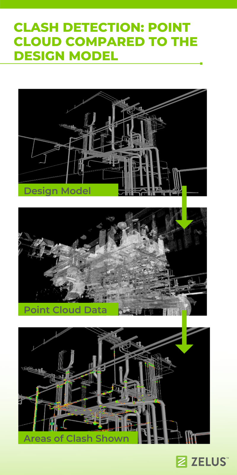
Several years ago, as part of QA/QC, our team developed an internal process for verifying the accuracy of the models we produced for clients. This process involved laying point cloud data [highly accurate existing condition] over the models we produced to identify where there were model omissions or deviations. This allowed us to deliver highly accurate as-builts–in 3-dimensional forms.
We quickly realized, however, this had applications beyond our four walls. What is now known as “Z Verify” is used in semiconductor, manufacturing, retail and distribution centers in several ways. One is to create highly accurate models that are used to inform designs and construction decisions prior to construction. The other is during construction to ensure what is actually being built stays true to the coordinated or design model.
Naturally, both of these applications are useful in semiconductor manufacturing, whether retooling an existing facility or building new.
A case study in semiconductor
Recently, a major chip manufacturer needed a digital as-built of one of their 10,000+ square-foot plants to plan for reconstruction. Using the Z Verify process, we completed a scan of the facility and compared the point cloud data with a previous model they had. The comparison revealed a number of elements that were missing from the model as well as deviations and errors.
(These are indicated in the magenta, yellow, and red colors below.)
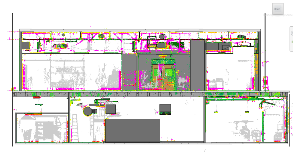
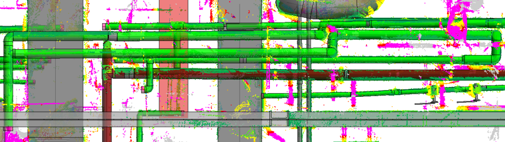
With this insight, they were able to make more informed design decisions before starting the construction process. Rather than encounter surprises during construction, they could plan to better mitigate issues and avoid unnecessary downtime. This data could also be used to prefabricate some of the elements off-site and ensure an easy install when the components arrived.
Another scenario involves an active construction site in which our team is currently using the Z Verify process as installation is occurring. This allows the design/build team to compare what’s actually being constructed with the coordinated model and make corrections before they become an issue. It also holds crews more accountable as errors can be traced back to the responsible party and corrected before construction progresses.
Using digital twins and the Z Verify process has the potential to change the way construction occurs. With the current cost of materials, and supply chain and labor shortages, construction teams and owners can’t afford unnecessary delays and rework. Z Verify is one way to circumvent that. And in semiconductor, it ensures what was intended to be built is actually built, and provides continuous QA/QC of tool installation.